SemiconductorX > Fab & Assembly > Packaging Equipment > Hybrid Bonding
WFE Hybrid Bonding Equipment
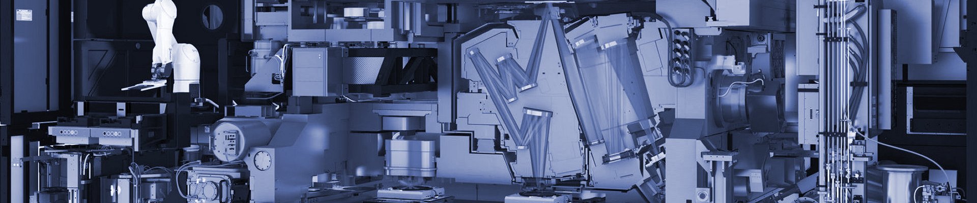
Hybrid bonding is the single most strategically significant packaging equipment category in production today. The technology enables direct copper-to-copper and oxide-to-oxide bonding between adjacent dies at sub-10 micrometer pitch — roughly 5× tighter than the microbump interconnects it replaces — and it is the gating technology for the most advanced products in multiple downstream segments simultaneously. HBM4 memory stacks transitioning from microbump to hybrid bonding architecture for base-die-to-DRAM interconnect. Foveros Direct at Intel for flagship compute die 3D integration. SoIC (System on Integrated Chips) at TSMC for 3D logic stacking. SAINT at Samsung Foundry. Advanced CoWoS-L with bridge dies. Every one of these flagship advanced packaging architectures depends on hybrid bonding equipment that exists effectively as a two-vendor duopoly between Besi (BE Semiconductor Industries, Netherlands) and Applied Materials, with emerging third-party capability at EV Group and Tokyo Electron.
The strategic concentration is structurally parallel to ASML's monopoly in EUV lithography. One specialty tool category where a narrow vendor base controls access to the capability that enables the most advanced products across memory, logic, and AI accelerators. Hybrid bonding equipment production cycle times are comparable to advanced lithography — roughly 12 to 18 months from order to installation — which means capacity for 2026–2028 hybrid bonding demand is already being set by tool orders being placed today. Whether the installed base of hybrid bonding equipment can scale fast enough to meet HBM4 and advanced AI accelerator 3D integration demand is one of the defining packaging supply chain questions of the next three years.
The Technology — Direct Copper-Oxide Bonding
Hybrid bonding creates permanent electrical and mechanical connections between two wafers (or between dies and a wafer) without solder, underfill, or specialty adhesives. The technology relies on the surface chemistry of copper and silicon dioxide to form atomic-scale bonds when two precisely prepared surfaces are brought into contact and subjected to specific thermal processing. The process operates on four distinct steps that the hybrid bonding equipment must execute in sequence or as an integrated flow.
Surface preparation. Both surfaces to be bonded — whether wafer-to-wafer or die-to-wafer — must be prepared with extreme planarity and cleanliness. The surfaces present an alternating pattern of copper pads (electrical contacts) and silicon dioxide (mechanical anchor). Surface roughness must be controlled to angstrom-scale (sub-nanometer), achieved through specialty CMP (chemical mechanical planarization) at the wafer preparation step. Particle contamination must be near-zero — a single particle of 100 nanometer diameter can prevent bonding across a wafer-scale region.
Activation. The oxide surfaces are activated via plasma treatment to create dangling hydroxyl groups that facilitate oxide-to-oxide bonding when surfaces contact. The plasma activation step is time-sensitive — activated surfaces degrade within hours if not bonded.
Alignment and contact. The two surfaces must be aligned to sub-100 nanometer accuracy (for sub-10µm pitch bonding; sub-50 nanometer for advanced applications) and brought into intimate contact across the entire bonding area. At this step the oxide-to-oxide bond initiates immediately through van der Waals forces.
Thermal processing. The bonded assembly is subjected to thermal processing (typically 150–400°C) to drive copper diffusion across the bond interface, completing the electrical connection between opposing copper pads. The thermal step is where hybrid bonding's distinctive advantage manifests — the final bond has electrical conductivity comparable to bulk copper, with no solder joints or intermetallic layers.
The integrated result is a bond that combines mechanical integrity (oxide-to-oxide bond) with electrical conductivity (copper-to-copper bond) across a wafer-scale or die-scale area. The sub-10µm pitch enables interconnect density approximately 25 times higher than microbump (~50µm pitch) and approximately 400 times higher than wire bond (~100µm pitch). The electrical characteristics — low resistance, low capacitance, excellent thermal conductivity — exceed those of any other packaging interconnect technology in production.
Why Hybrid Bonding Matters — The Enabling Applications
Hybrid bonding's commercial significance derives from the specific products it enables that cannot be produced at comparable performance with microbump alternatives. Understanding these applications is essential to understanding why hybrid bonding equipment capacity matters at industry scale.
HBM4 memory stacks. The transition from HBM3e (microbump-based) to HBM4 (hybrid-bonding-based) is the largest volume hybrid bonding application in the industry. HBM4 specifications require the base-die-to-DRAM interconnect density that only hybrid bonding delivers at the target 2048-bit interface width. SK hynix, Samsung Memory, and Micron are qualifying hybrid bonding for HBM4 production, with first commercial shipments projected 2026. HBM4 volume demand is tied directly to AI accelerator production — every NVIDIA Rubin-class GPU, AMD MI400-class accelerator, and hyperscaler custom AI accelerator uses HBM4 at scale.
Foveros Direct at Intel. Intel's advanced 3D packaging platform uses hybrid bonding for compute die stacking at sub-10µm pitch. Foveros Direct is Intel's answer to TSMC SoIC and Samsung SAINT, and flagship Intel products including Ponte Vecchio, Clearwater Forest, and future Core/Xeon generations use or will use Foveros Direct. Intel's captive hybrid bonding capacity at US fabs (Hillsboro, Arizona) is a specific strategic investment.
SoIC at TSMC. TSMC's System on Integrated Chips platform integrates multiple dies vertically using hybrid bonding. SoIC enables chiplet architectures at TSMC that compete with Intel Foveros and Samsung SAINT. AMD MI300-series and MI400-series accelerators use TSMC SoIC for their compute die stacking. TSMC SoIC capacity at Taiwan is the reference 3D IC capacity globally.
SAINT at Samsung Foundry. Samsung's answer to SoIC and Foveros, using hybrid bonding for 3D die stacking at Samsung Foundry customers. SAINT is earlier in ramp than SoIC or Foveros Direct but is strategically important for Samsung's foundry competitiveness.
Advanced CoWoS-L with bridge dies. CoWoS-L (with local silicon interconnect bridge dies) uses hybrid bonding at the bridge-to-main-die interface for highest-bandwidth applications. NVIDIA Blackwell-generation and future GPUs use advanced CoWoS-L with hybrid bonding for specific interconnect tiers.
The common thread across these applications is that each represents the most advanced product tier in its segment — flagship memory (HBM4), flagship CPUs and AI accelerators (Intel Foveros Direct, TSMC SoIC, Samsung SAINT), and flagship AI integration platforms (advanced CoWoS-L). Hybrid bonding is the technology that distinguishes the flagship tier from the mainstream tier. When hybrid bonding capacity is constrained, the flagship tier products are directly gated.
The Besi-Applied Materials Duopoly
Besi (BE Semiconductor Industries, Duiven, Netherlands) operates the industry reference hybrid bonding platform. The Besi 8800 Ultra Plus system is the hybrid bonder installed at leading operators globally — TSMC, Samsung, Intel, SK hynix, Samsung Memory, Micron — for advanced packaging and HBM production. Besi's hybrid bonding development began in the early 2010s, well before the category reached commercial significance, and Besi has benefited from substantial first-mover advantage in tool architecture, customer qualification, and installed-base operational experience. The 8800 Ultra Plus offers sub-100 nanometer alignment accuracy, integrated thermal processing, and production-scale throughput suitable for volume HBM and 3D IC manufacturing.
Applied Materials (Santa Clara, California) operates hybrid bonding capability through its advanced packaging business, which includes both direct Applied Materials hybrid bonding systems and integrated 3D packaging platforms that combine Applied Materials wafer processing with Besi bonding capability. The Applied-Besi relationship has been both partnership and competitive over time. Applied Materials has been developing captive hybrid bonding capability to complement its broader advanced packaging equipment portfolio. For Applied Materials customers, the integrated advanced packaging flow — wafer preparation, surface activation, bonding, post-bond processing — spans the Applied Materials tool portfolio more completely than at Besi, which has historically been the specialty bonder vendor.
The competitive dynamic between Besi and Applied Materials reflects their different origins. Besi approached hybrid bonding from back-end packaging — extending die attach and flip-chip bonding expertise into wafer-scale hybrid bonding. Applied Materials approached hybrid bonding from front-end wafer processing — extending CMP, etch, and deposition expertise into wafer-bonding applications. Both approaches have produced viable hybrid bonding platforms, and customers have qualified both in different applications. SK hynix has been associated with Besi hybrid bonding for HBM4 development; Samsung has qualified both vendors; TSMC uses Besi extensively for SoIC; Intel has internal hybrid bonding development with partnerships across both Besi and Applied Materials.
Neither vendor has disclosed complete production capacity data publicly, but industry estimates suggest Besi leads in installed base by a modest margin while Applied Materials has larger potential capacity growth given its broader manufacturing footprint. Together they represent essentially the entire production-scale hybrid bonding capacity globally.
Emerging Third-Party Capability
Credible third-party hybrid bonding capability is emerging from two sources, though both remain smaller than Besi or Applied Materials at production scale.
EV Group (EVG, Sankt Florian, Austria) is the global wafer bonding specialist with deep expertise in wafer-to-wafer bonding across SOI substrates, MEMS wafer bonding, and specialty advanced packaging applications. EVG has extended this expertise into hybrid bonding platforms that target specific customer applications. EVG's positioning is particularly strong in research and pilot-line engagements, where EVG's wafer bonding heritage and customer relationships support early hybrid bonding qualification work. At volume production scale, EVG's hybrid bonding position has been smaller than Besi or Applied Materials, but EVG's wafer bonding installed base provides a foundation for capacity growth if customer demand materializes.
Tokyo Electron (TEL) has announced hybrid bonding platforms as part of its broader advanced packaging equipment strategy. TEL's positioning leverages its existing WFE (wafer fab equipment) relationships at TSMC, Samsung, and Intel — customers that are also the primary hybrid bonding equipment buyers. TEL's hybrid bonding development has been in progress for several years, with first production-scale deployments projected mid-decade. If TEL achieves production-scale hybrid bonding capability, it becomes the credible third vendor that diversifies the supply beyond the Besi-Applied duopoly.
Chinese domestic hybrid bonding equipment development is underway at specialty operators including NAURA, ACM Research, and specialty advanced packaging tool developers. The Chinese capability gap against Besi and Applied Materials is substantial — hybrid bonding is one of the most demanding packaging equipment categories in precision engineering, and the installed-base learning curve at Besi and Applied Materials represents years of operational experience that domestic alternatives cannot readily replicate. Export restrictions on advanced Chinese packaging equipment further constrain Chinese operator access to Besi and Applied Materials tools for advanced applications. Chinese hybrid bonding capability at mature applications is feasible on longer timescales but advanced-pitch hybrid bonding (sub-10µm, sub-micron) remains structurally concentrated at Western and Japanese tool suppliers.
Cost, Delivery Cycles, and Capacity Economics
Hybrid bonding equipment cost structure reflects its specialty positioning at the high end of packaging equipment. A single Besi 8800 Ultra Plus or equivalent Applied Materials hybrid bonder costs approximately $5 to $10 million or more in advanced configurations — the most expensive per-unit packaging tool outside of wafer bonding systems for very large-format applications. Complete hybrid bonding lines at a production facility require multiple bonders plus specialty wafer preparation, inspection, and post-bond processing equipment — a complete hybrid bonding line can reach $50 to $100 million in total tool CapEx.
Delivery cycles are substantial. From tool order to installation typically runs 12 to 18 months at current demand levels, with the lead time sensitive to category-specific capacity and customer qualification requirements. This means that hybrid bonding capacity for 2027 production must be ordered in late 2025 to 2026; capacity for 2028 must be ordered in 2026 to 2027. The multi-year ordering horizon creates specific capacity planning risk — if HBM4 ramp or advanced AI accelerator demand outpaces tool delivery, capacity shortfalls cannot be rapidly remediated.
Operational economics favor high utilization. Hybrid bonders are capital-intensive tools that must run at high utilization to amortize their capital cost. Downtime from tool qualification issues, consumable replacement, or process excursions directly affects operator economics. High-volume hybrid bonding operations at SK hynix HBM4 lines, TSMC SoIC lines, Intel Foveros Direct lines require continuous production with minimal unplanned downtime — a requirement that reinforces vendor-customer operational relationships over time.
The Capacity Constraint Framework
Hybrid bonding capacity is one of the most visible binding constraints in AI accelerator production. The constraint can be analyzed at multiple tiers.
Memory IDM hybrid bonding capacity — SK hynix, Samsung Memory, and Micron each operate captive hybrid bonding lines for HBM4 production. HBM4 demand is doubling approximately annually with AI accelerator volume growth; hybrid bonding capacity at the memory IDMs must scale in parallel. Each memory IDM operates multiple hybrid bonders at each HBM4 production facility; specific capacity numbers are not publicly disclosed but are tracked closely by industry observers and AI accelerator customers.
Foundry captive hybrid bonding capacity — TSMC, Samsung Foundry, and Intel each operate captive hybrid bonding lines for SoIC, SAINT, and Foveros Direct production respectively. These lines serve flagship compute die integration for external customers (TSMC, Samsung Foundry) and internal products (Intel). Advanced CoWoS-L with bridge dies uses TSMC captive hybrid bonding capacity additionally.
Tool capacity at Besi and Applied Materials — the upstream constraint on how rapidly memory IDM and foundry captive hybrid bonding capacity can expand. Besi and Applied Materials production capacity determines the maximum rate at which new hybrid bonders can be built and delivered. Both vendors have announced substantial capacity expansions to meet demand, but tool production itself requires specialty engineering talent, specialty components, and manufacturing capacity that cannot be expanded faster than physical constraints allow.
The cascading constraint chain — AI accelerator demand → HBM4 demand → HBM4 test capacity (at Advantest ATE) → hybrid bonding capacity (at memory IDMs and foundries) → hybrid bonding tool delivery (at Besi and Applied Materials) — means any single tier becoming a bottleneck propagates through to AI accelerator shipment. Hybrid bonding capacity has been identified by industry observers as a specific vulnerable tier in this chain, given the long tool delivery cycles and narrow vendor base. See Bottleneck Atlas for the integrated supply chain chokepoint framing.
Related Coverage
Parent: Packaging Equipment
Peer packaging equipment categories: Flip-Chip Bonding · Wire Bonding · Die Attach · Wafer Dicing · Molding & Encapsulation
Enabling applications: HBM (HBM4 hybrid bonding transition) · Foveros (Foveros Direct) · SAINT (Samsung 3D stacking) · CoWoS (advanced CoWoS-L bridge) · 3D IC · Advanced Interconnects
Related packaging equipment topics: Advanced Packaging Inspection & Metrology (hybrid bonding interface verification) · CMP (surface preparation at sub-nanometer planarity)
Operators and facilities: Foundry Captive Packaging (TSMC, Samsung, Intel hybrid bonding lines) · IDM Captive Packaging (memory IDM HBM4 hybrid bonding)
Vendor profiles (planned): Besi · Applied Materials · EV Group · Tokyo Electron
Cross-pillar strategic framing: AI Accelerators (hybrid bonding as binding constraint) · Bottleneck Atlas