SemiconductorX > Fab & Assembly > Test Equipment > Probe Cards
ATE Probe Cards
Probe cards are the specialized electrical interface between Automated Test Equipment (ATE) and the wafer at wafer-level probe test. A probe card contains thousands of micro-contacts (cantilever beams, vertical spring-loaded probes, or MEMS-style probe tips) that make momentary electrical contact with the bond pads of each die on a wafer during test, enabling the ATE to apply test vectors and measure device responses before the wafer is diced into individual packaged parts. Probe cards are custom-designed per product — there is no generic probe card — and they are consumable, wearing out after a predictable number of touchdowns (typically hundreds of thousands to millions of test contacts) and requiring replacement. A high-volume modern test operation consumes thousands of probe cards annually, making probe card supply a volume commodity consumable rather than a one-time capital purchase.
The probe card industry is oligopolistic with four to six major vendors serving different segments. FormFactor (Livermore, California) is the global leader with broad product portfolio, operating across logic, memory, and specialty applications. The 2016 acquisition of Cascade Microtech expanded FormFactor's position into specialty RF and analog probe applications. Technoprobe (Cernusco Lombardone, Italy) has grown substantially over the past decade, particularly in high-performance logic probe cards for advanced-node applications at TSMC, Samsung, and Intel leading-edge customers. Japan Electronic Materials (JEM) has specialty strength at Japanese customers and in specific probe card categories. Micronics Japan, MPI (Taiwan), and specialty Asian operators serve specific segments. Chinese domestic probe card capability exists at mature applications but faces substantial gaps at advanced-node and HBM-specific probe card applications.
Probe cards are one of the less-discussed specialty supply chains in semiconductor equipment. Unlike ATE (which is purchased as capital equipment and receives industry attention as major tool investments) probe cards are consumables that flow continuously into high-volume test operations. Unlike EUV (which has visible industry significance as the ASML monopoly) probe cards are dispersed across multiple specialty vendors. But advanced-node probe cards and HBM-specific probe cards represent specific concentrations of capability — supplier selection for these applications affects test throughput and yield directly, and supply chain disruption at the key suppliers would propagate to test operations quickly.
Probe Card Technology and Architecture
Probe card technology has evolved through multiple generations of contact architecture, each responding to specific requirements of the devices being tested. Understanding the architecture types matters because different architectures serve different applications.
Cantilever probe cards use thin metal beams extending from a substrate to contact bond pads. Each cantilever acts as a spring that deflects when contact is made, providing controlled contact force. Cantilever probe cards have been the workhorse for mature and mid-range applications for decades. The architecture is well-characterized, cost-effective at moderate pitch, and reliable for typical logic and mixed-signal test. Cantilever probes have practical limits at tight-pitch advanced-node applications where beam stiffness and alignment become challenging below approximately 60–80µm pitch.
Vertical probe cards use spring-loaded vertical probe pins that contact bond pads from above. The vertical architecture enables tighter pitch than cantilever probes (down to 40–50µm) and better electrical characteristics for high-frequency applications. Vertical probes have become the mainstream architecture for advanced SoC test at most leading applications. The spring mechanism requires specific design to maintain controlled contact force across many thousands of pins simultaneously.
MEMS probe cards use micro-fabricated probe structures produced via MEMS (microelectromechanical systems) processes. MEMS probe cards enable extreme tight-pitch applications (sub-40µm, sub-20µm for advanced applications) through precise photolithographic definition of probe tip geometry. MEMS probe cards have become essential for advanced-node logic test and HBM stack test where pitch requirements exceed what vertical probes can reliably achieve. FormFactor, Technoprobe, and specialty operators have invested substantially in MEMS probe card capability.
Specialty RF and high-frequency probe cards optimize electrical characteristics for high-frequency signal integrity — matched impedance across channels, controlled crosstalk, controlled insertion loss at GHz-class signal frequencies. These specialty applications serve RF IC test, high-speed serializer-deserializer (SerDes) test, and specialty applications where signal integrity dominates over pitch or pin count considerations.
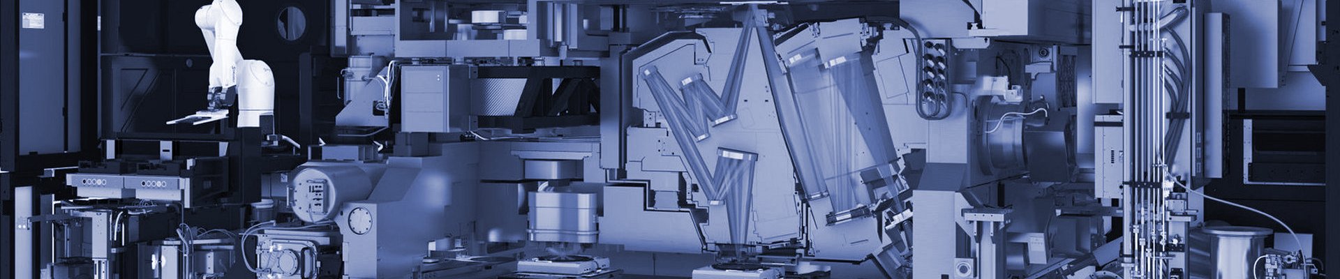
A modern advanced-node probe card combines multiple architecture elements — MEMS probe tips for pitch, vertical spring mechanisms for contact force, specialty impedance-controlled routing for signal integrity, thermal management substrates for temperature stability. The integrated probe card is a precision engineered assembly of thousands of individual components, and the engineering difficulty increases substantially with each advance in device complexity.
Custom Per-Product Design and Test Program Integration
Every probe card is custom-designed for a specific device under test. The probe card's pin layout must match the bond pad layout of the specific die; the probe card's electrical channels must match the test pattern signal assignments defined in the test program; the probe card's mechanical geometry must match the wafer prober and the device package dimensions. A new product introduction at a customer — whether a new NVIDIA GPU generation, a new SK hynix HBM generation, or a new automotive MCU product family — requires a new probe card design specific to that product.
Probe card design cycles typically run 3 to 6 months from initial specification to first production cards, longer for advanced-node applications or complex HBM stacks. The design process involves close collaboration between the probe card vendor's engineering team, the customer's test engineering team, and the ATE vendor's applications engineering. Probe card qualification at the customer involves correlation testing (comparing probe card measurement results to reference measurements), yield validation, and throughput characterization. Only after qualification does production volume of the probe card ramp.
The engineering intensity per probe card design is substantial. FormFactor, Technoprobe, and JEM maintain large engineering organizations dedicated to probe card design — hundreds of engineers across each major operator. The engineering workload scales with customer product introduction rates; when customers launch more products, probe card engineering demand grows correspondingly. This engineering intensity creates a natural barrier to new entrants at advanced-node applications — a new operator cannot quickly build the engineering capability to serve TSMC, Samsung, or leading memory IDM customers at advanced applications.
The Consumable Economics
Probe cards are consumables that wear out through repeated contact with wafer bond pads. Typical wear lifetimes are hundreds of thousands to low millions of touchdowns per probe card, with specific lifetime depending on contact force, bond pad metallurgy, and probe tip material. High-volume test operations — where a single probe card might test hundreds or thousands of wafers per day — consume probe cards on predictable replacement cycles. Budgeting probe card consumption is a specific operational concern for test operators.
Probe card cost varies dramatically across applications. Basic cantilever probe cards for commodity applications can cost $50,000 to $200,000 per card. Advanced vertical or MEMS probe cards for leading-edge applications cost $500,000 to $2,000,000 or more per card in the highest-capability configurations. HBM-specific advanced probe cards for leading HBM4 test applications are at the high end of the cost range. The annual probe card consumption at a high-volume HBM4 test operation can reach tens of millions of dollars in probe card replacement cost alone.
The consumable economics distinguish probe cards from most other test equipment categories. ATE is a one-time capital purchase amortized over 15 to 25 year tool lifetimes. Handlers, wafer probers, and specialty burn-in equipment are similarly long-lived capital assets. Probe cards are continuously replenished operational inputs, comparable to photomasks at wafer fabs or consumable chemicals at advanced packaging. This operational flow means probe card supply chain stability — steady production at the key vendors, predictable delivery times, reliable quality — directly affects day-to-day test operations.
Advanced-Node and HBM Probe Cards — The Specialty Concentration
Probe card supply is increasingly concentrated at specific advanced applications even as the broader probe card market remains distributed across multiple vendors. Two specific application categories have become specialty concentrations of capability.
Advanced-node logic probe cards (for sub-5nm logic devices). Devices at N3, N2, and future logic nodes have specific probe card requirements — tight-pitch bond pad layouts (sub-40µm), high-density I/O counts (2,000+ pins per die for flagship SoCs), high-frequency signal integrity requirements, and thermal stability during test. FormFactor and Technoprobe have been competing intensively for design wins at TSMC, Samsung Foundry, and Intel leading-edge customers. The engineering capability required for advanced-node probe cards takes years to develop, creating a natural concentration of capability at these two primary vendors. JEM and specialty vendors serve specific applications but the advanced-node volume concentration is at FormFactor and Technoprobe.
HBM probe cards (for stacked memory test). HBM stack testing requires probe cards capable of contacting the high-pin-count, tight-pitch micro-bump interfaces that connect HBM stacks to test equipment. HBM3 and HBM4 probe cards at the memory IDMs and at merchant HBM test operators (KYEC and specialty test houses) represent specific engineering capability. The combination of tight pitch, high pin count, high-speed signaling, and stack-alignment requirements makes HBM probe cards among the most demanding probe card applications in production. Capacity constraint at HBM probe card supply can bind HBM test throughput — with HBM demand doubling annually, probe card capacity at the HBM-qualified suppliers is a specific capacity planning concern.
The combined concentration at advanced-node logic probe cards and HBM probe cards represents the strategic intersection of the probe card industry with the broader AI accelerator supply chain. Both FormFactor and Technoprobe have invested substantially in capacity expansion for these specialty applications.
Vendor Landscape in Detail
FormFactor (Livermore, California) is the global probe card leader with revenue approximately $700 million and broad positioning across logic, memory, and specialty applications. FormFactor's 2016 acquisition of Cascade Microtech added specialty RF and analog probe capability. The company has invested substantially in MEMS probe card development for advanced-node applications and has design wins at TSMC, Samsung, Intel, and the memory IDMs. FormFactor's customer base includes both major memory and logic operators, providing diversified revenue across the probe card market segments.
Technoprobe (Cernusco Lombardone, Italy) has grown to be the primary competitor to FormFactor at advanced-node applications. The company's capability in vertical and MEMS probe cards has established strong positions at TSMC and Samsung for advanced-node logic applications. Technoprobe went public in 2022 and has continued substantial engineering capability investment. The company's positioning is more focused on advanced-node logic than FormFactor's broader portfolio — a focused-specialist strategy that has enabled deep capability development.
Japan Electronic Materials / JEM (Tokyo, Japan) serves specialty applications at Japanese customers and in specific probe card categories. JEM has historical strength at Renesas, Kioxia, and Japanese specialty operators for automotive MCU and memory test applications. The company's scale is smaller than FormFactor or Technoprobe but its specialty positioning at Japanese customers provides structural stability.
Micronics Japan (Tokyo, Japan) serves specialty probe card applications with particular strength in memory test and specific Japanese customer applications.
MPI (Taiwan) operates in both probe cards and wafer probers, serving specialty Taiwan and Asian customers. MPI's capability is particularly in specific commodity and mid-range applications.
Chinese domestic probe card operators including specialty Chinese vendors serve mature Chinese test applications at commodity microcontrollers, mature SoCs, and specific test applications. The capability gap at advanced-node and HBM probe cards is substantial — Chinese domestic probe card capability at flagship applications is years behind FormFactor and Technoprobe, and closing the gap requires substantial engineering capability development plus access to specific MEMS process capability that US and allied export controls increasingly restrict.
Operational Challenges and Engineering Intensity
Probe card operations face specific operational challenges that differentiate them from other test equipment segments.
Engineering cycle time. New probe card designs require 3–6 months minimum from specification to delivery, longer for complex applications. When a customer introduces a new product, probe card development is on the critical path for production test readiness. Customer product roadmap changes or accelerations can stress probe card vendor engineering capacity.
Small-lot manufacturing. Each probe card design is produced in relatively small lots — perhaps dozens to hundreds of probe cards per design over the design's production life. This small-lot manufacturing is less suited to conventional semiconductor fab economics and more aligned with specialty precision manufacturing. The probe card vendors operate specialty manufacturing capabilities tuned for small-lot precision production.
Variability management. Individual probe cards within the same design batch may have subtle variations in electrical characteristics. Characterizing and managing these variations is a significant operational concern — customer test engineering must account for probe-card-to-probe-card variation in test program development and yield analysis.
Repair and refurbishment. Worn probe cards can sometimes be refurbished (probe tip replacement, contact cleaning, recalibration) rather than disposed. Refurbishment capability at the vendor or at specialized third-party refurbishment operators extends effective probe card life and reduces consumable cost.
Related Coverage
Parent: Test Equipment
Peer test equipment categories: ATE (Automated Test Equipment) (probe cards connect to ATE) · Wafer Probers (probe cards mount on probers) · Handlers · SLT
Test discipline coverage: Advanced Packaging Test · Final Test
Applications with probe card specialty concentration: HBM (HBM probe card concentration) · AI Accelerators (advanced-node probe cards at flagship applications) · Leading-Edge Logic (N3, N2 probe card requirements)
Operators and facilities: Standalone Test Houses (consumable probe card demand at merchant test) · Foundry Captive Packaging · IDM Captive Packaging
Vendor profiles (planned): FormFactor · Technoprobe · Japan Electronic Materials · Micronics Japan