SemiconductorX > Fab & Assembly > Test Equipment > ATE
ATE (Automated Test Equipment)
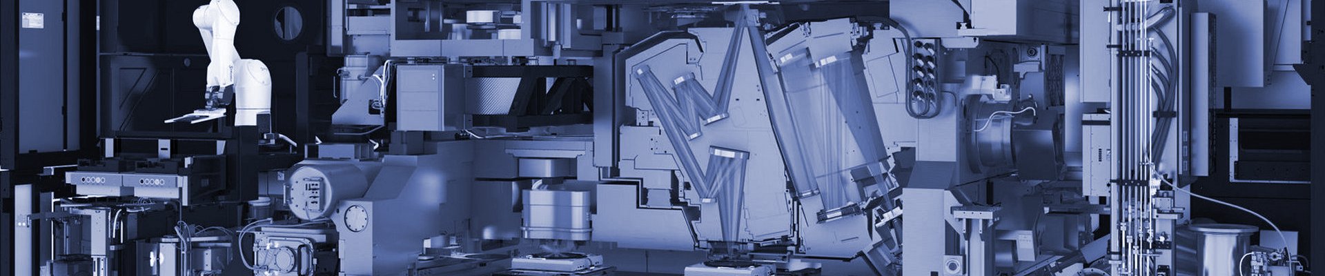
Automated Test Equipment (ATE) is the foundation of semiconductor testing — the large-scale electrical test systems that apply millions of test vectors per device, measure the device responses, and identify defective parts. Every semiconductor that ships passes through ATE at least once (at wafer probe or at final package test, often at both), and many pass through multiple ATE platforms across the production flow. The ATE market is a two-operator duopoly between Advantest (Tokyo, Japan) and Teradyne (North Reading, Massachusetts), together controlling approximately 80% or more of the global ATE market by revenue. The duopoly has been stable for approximately two decades. Specialty ATE vendors serve specific applications — Cohu for memory-related test systems, Chroma ATE (Taiwan) for LED and display driver test, and various regional operators — but the core digital and memory ATE market remains concentrated at Advantest and Teradyne.
The duopoly has distinct product specializations. Advantest operates the V93000 as its flagship single-platform ATE architecture, with particular strength in memory testing and HBM testing. The V93000 is the industry reference for memory test at SK hynix, Samsung Memory, and Micron, and Advantest has leveraged this memory strength into the dominant position in HBM4 test. Teradyne operates a broader portfolio — FLEX and UltraFlex for advanced SoC test, Eagle Test Systems for specialty applications, and J750 for high-volume microcontroller and commodity device test. Teradyne has historical strength in SoC test (mobile application processors, automotive SoCs, networking chips) and has expanded substantially into system-level test (SLT) and AI accelerator test capabilities.
What ATE Does
An ATE system applies electrical test patterns — sequences of input signals — to a device under test (DUT) at controlled timing and voltage levels, and measures the resulting output signals to verify that the device produces expected behavior. The test patterns are generated either from the device's logical design (via automated test pattern generation / ATPG tools that produce patterns to exercise specific transistors and logic gates) or from specific functional test scenarios. Modern ATE platforms can apply test vectors at hundreds of megahertz to gigahertz rates, test thousands of pins simultaneously, and execute complex test programs combining many thousand individual measurements per device.
ATE capability spans multiple dimensions:
Pin count. Advanced ATE platforms provide thousands of test channels (pins) connected to the device under test. A modern advanced-node SoC with 2,000+ I/O pins requires ATE with matching or greater channel count. HBM stacks with hundreds of high-speed data pins plus signaling, clock, and power pins require high-pin-count ATE configurations.
Data rate. Test vector application rates have scaled with device operating speeds. Legacy ATE operated at tens of MHz; modern advanced ATE operates at GHz-class data rates. HBM4 testing at 8 Gbps+ per channel requires ATE capable of applying and measuring at these rates across many parallel channels simultaneously.
Voltage and timing precision. ATE must apply input signals at precisely controlled voltage levels and time instants, and measure output signals with matching precision. Timing accuracy below 10 picoseconds and voltage accuracy below 1 millivolt are required at leading-edge applications. Measurement uncertainty directly affects test yield — imprecise ATE may fail good parts or pass bad parts.
Test coverage. The ATE test program determines what fraction of device functionality and defects are tested. Structural test (ATPG-derived) tests the underlying circuit connectivity; functional test exercises device behavior under realistic operating conditions; specialty tests (memory cell test, analog characterization, scan test, BIST validation) cover specific aspects. Test coverage scales with test time and ATE capability.
Multi-site testing. Modern ATE can test multiple devices simultaneously in parallel sites. High-volume commodity test operates with dozens to hundreds of devices tested in parallel on single ATE systems; advanced applications test fewer sites per system but with more complex per-site measurement.
Advantest V93000 — The Memory and HBM Reference
The Advantest V93000 is a single-architecture ATE platform that has been the industry reference for memory testing for over a decade. The platform's success derives from several engineering characteristics. The V93000 uses a modular "pin scale" architecture where different test capabilities (digital, analog, RF, power) can be configured in specific test slots — enabling a single platform to serve a wide range of applications. The platform has deep operational history at the memory IDMs, with continuous software and hardware evolution over the platform's life.
The V93000's HBM test dominance is particularly significant. HBM4 testing requires specialty capability — high-pin-count (2048-bit interface width plus control), high-speed (8 Gbps+ per channel), and complex protocol validation (JEDEC HBM4 specification conformance). The V93000 has been qualified and deployed for HBM4 test at SK hynix, Samsung Memory, and Micron's HBM production lines. Advantest's operational relationships with the memory IDMs and with NVIDIA on HBM test architecture (since NVIDIA is the dominant HBM consumer) have established the V93000 as the near-exclusive ATE platform for HBM test at scale.
Beyond HBM, the V93000 serves broad memory test applications — DRAM cell testing, NAND flash testing, embedded memory validation in SoCs, specialty memory IP verification. The platform also serves specific logic test applications, particularly where the V93000's configuration flexibility aligns with customer requirements. Advantest's SLT (system-level test) platforms extend the V93000 architecture into AI accelerator and specialty SLT applications.
Teradyne — FLEX, UltraFlex, Eagle, and J750
Teradyne's ATE portfolio spans several platforms with different application targets, reflecting Teradyne's strategy of specialty platforms rather than Advantest's single-platform approach.
UltraFlex is Teradyne's flagship advanced SoC test platform. Used extensively for mobile application processors, advanced CPUs, networking SoCs, and specialty logic. UltraFlex has been the reference Teradyne platform at Apple's iPhone mobile processor test flow for multiple generations, with operational depth at Apple's test partners and Apple's internal test organization. UltraFlex has also seen deployment for AI accelerator test, particularly at Teradyne-qualified AI accelerator customers.
FLEX is the predecessor platform (still in production use at many customers) covering broad digital SoC test applications at data rates and complexity levels below UltraFlex. FLEX serves mature and mid-range SoC products where UltraFlex capability exceeds requirements and cost considerations favor the older platform.
Eagle Test Systems is Teradyne's specialty platform acquired via the 2008 Eagle acquisition. Eagle serves specific applications in power management, specialty analog, and mixed-signal testing where Eagle's specific analog capability is differentiated.
J750 is Teradyne's high-volume commodity microcontroller test platform. Used extensively for automotive MCUs, industrial MCUs, consumer microcontrollers, and specialty commodity products. The J750 has been the workhorse Teradyne platform at OSATs (ASE, Amkor, JCET) and at captive test operations for volume commodity products. The J750 has been in production for decades with continuous incremental improvement — a pattern that contrasts with the generational replacement cycles at more advanced platforms.
Teradyne's strategic positioning has emphasized broader portfolio breadth versus Advantest's V93000 single-platform concentration. Teradyne's customer base includes Apple (UltraFlex for mobile processors), AMD (UltraFlex and specialty platforms for CPUs and GPUs), Qualcomm (mobile and infrastructure test), automotive IDMs (J750 and specialty platforms), and broad industrial and consumer semiconductor operators.
Logic Test versus Memory Test
The ATE market divides at a fundamental level between logic test and memory test. Understanding the distinction matters because operator specializations, platform architectures, and market dynamics differ between the two.
Logic test covers digital SoCs, microcontrollers, GPUs, AI accelerators, and other logic devices. Test patterns are derived from the device's logical design via ATPG, with scan-chain infrastructure in the device enabling structural defect coverage. Functional tests exercise specific behaviors. Logic test typically runs from seconds to minutes per device depending on device complexity. Logic ATE requires broad coverage across digital, mixed-signal, and specialty test capabilities. Teradyne has historical strength in logic test; Advantest V93000 also serves logic test applications.
Memory test covers DRAM, SRAM, NAND flash, HBM, and specialty memory devices. Test patterns exercise memory cell behavior — reading and writing specific patterns, verifying data retention, testing specific refresh and timing parameters. Memory test at full coverage can require hours per DRAM chip or HBM stack at advanced configurations. Memory ATE requires specialty capability in timing precision, high-pin-count at high data rates, and specific memory protocol validation. Advantest V93000 is the dominant memory test platform; Teradyne has memory test capability but smaller market position.
HBM test specifically bridges both categories. HBM stacks are memory devices but they integrate base dies with logic functions, and HBM test requires capabilities spanning memory and logic domains simultaneously. HBM test has been the fastest-growing ATE segment over the past three years, driven by AI accelerator demand growth.
AI Accelerator Test Complexity
AI accelerators — NVIDIA H-series, B-series, and Rubin-class GPUs, AMD MI-series, Google TPU, hyperscaler custom AI silicon, emerging AI chipmakers — represent the most demanding ATE requirements in current production. Several factors drive this complexity.
Die size. AI accelerators are among the largest dies in production — NVIDIA B-series approaches 800 mm² or larger for the largest configurations. Large dies have more pins to test, more transistors to exercise, and more specific test conditions to verify. Test time per die scales roughly with die complexity.
Multi-die integration. AI accelerators use advanced packaging that integrates a primary compute die with HBM stacks, interposer routing, and specialty chiplets. Testing the integrated package requires coordinated test of the compute die and the HBM stacks plus verification of inter-die communication. Package-level test complements individual die test at the package-assembly stage.
Workload validation. AI accelerators are tested against actual AI inference and training workloads (via system-level test at Teradyne, Advantest, or Cohu SLT platforms) because pattern-based ATE testing cannot fully characterize behavior under realistic AI workloads. Workload test time can substantially exceed pattern-based test time.
Thermal sensitivity. AI accelerators operate at high power densities and are thermally sensitive — test systems must control die temperature precisely during test, often at multiple temperature conditions (cold test, room temperature test, hot test). Thermal control equipment integrated with the ATE is a specialty capability.
The aggregate result is that AI accelerator test time per device runs to hours, test capacity per ATE line is limited compared to commodity SoC test, and ATE capital cost per unit test time is substantially higher. AI accelerator test capacity scaling has been an operational challenge across the industry, driving expansion of test capability at Advantest and Teradyne advanced platforms as well as at SLT-specific systems from Cohu.
Chinese Domestic ATE
Chinese domestic ATE capability is scaling but remains structurally behind Advantest and Teradyne at advanced applications. Specialty Chinese ATE operators — including ChipWare and specialty operators focused on specific test applications — serve mature-node Chinese test with capability in commodity microcontrollers, mature SoCs, and specialty test applications. Chinese capability at advanced SoC test (equivalent to Teradyne UltraFlex), advanced memory test (equivalent to Advantest V93000 for HBM), and AI accelerator test (equivalent to the leading Western platforms) is the specific gap that Chinese domestic ATE cannot close quickly.
The Chinese ATE advancement trajectory parallels the broader Chinese semiconductor equipment advancement story — mature-node self-sufficiency achievable on feasible timescales, but advanced applications constrained by equipment design IP gaps, software tool gaps (ATPG tools are themselves concentrated at US and European vendors), and customer qualification cycles that favor incumbent platforms. US and allied export controls on advanced ATE exports to China further constrain Chinese advanced test equipment access.
HBM test specifically is the acute Chinese capability gap. CXMT and other Chinese memory operators that might eventually produce HBM-class products face a test equipment gap that existing Chinese domestic ATE cannot close. This gap compounds the Chinese HBM production advancement challenge alongside the previously-documented gaps in hybrid bonding equipment and advanced DRAM process capability.
ATE Cost Structure and Lifecycle
ATE tool costs scale with capability across a wide range. Commodity ATE at the Teradyne J750 tier costs approximately $1 to 3 million per system and operates across high test volumes of commodity devices. Advanced ATE at the UltraFlex and V93000 tiers costs approximately $5 to 15 million per system and targets advanced SoC and memory applications. HBM-specific advanced configurations at the high end approach $10 million or more per system. Complete test lines at major test operators can reach $50 to 200 million in ATE capital plus specialty probe cards, probers, and handlers.
ATE platforms operate over long lifecycles — 15 to 25 years or longer for successful platforms. The Teradyne J750 has been in production for over two decades with continuous evolution. The Advantest V93000 has been in production since 2000 with substantial architectural evolution. Long platform lifecycles favor customer depth — test engineering teams at major customers build multi-year expertise on specific platforms, and test program assets (test patterns, device-specific configurations, customer-specific debug infrastructure) accumulate over years of platform use. Switching ATE platforms is a substantial operational event.
Consumables and ongoing operational costs include specialty probe cards (see Probe Cards) which are distinct consumable items, maintenance contracts, software license renewals, and specialty test socket and contactor assemblies. These ongoing costs add 10% to 30% of annual ATE capital cost to operating expense.
Related Coverage
Parent: Test Equipment
Peer test equipment categories: Probe Cards (test interface to ATE) · Wafer Probers · Handlers · SLT (System-Level Test) · Burn-In Systems
Applications tested: HBM (V93000 dominant) · AI Accelerators (UltraFlex, V93000, SLT) · Automotive MCUs (J750) · NAND Flash (memory ATE)
Test discipline coverage: Advanced Packaging Test · Final Test
Operators and facilities: Standalone Test Houses · Foundry Captive Packaging · IDM Captive Packaging