SemiconductorX > Fab & Assembly > Wafer Fab Equipment > Lithography > ASML EUV Scanner
ASML EUV Scanner
The ASML Extreme Ultraviolet (EUV) lithography scanner is the single most strategically significant piece of semiconductor manufacturing equipment in the world. No other tool has comparable monopoly concentration, comparable downstream impact, or comparable geopolitical attention. ASML is the sole global supplier of EUV lithography — there is no viable competitive alternative at commercial scale, and no foreseeable path to one within the current decade. Every leading-edge logic fab in production today depends on ASML EUV scanners to define transistor and interconnect features at 7nm, 5nm, 3nm, and 2nm nodes. Every HBM-class DRAM production line at advanced D1x generations depends on EUV for cell capacitor and peripheral patterning. The monopoly was established through approximately three decades of research and development investment, billions of dollars in accumulated capability, and a specific vendor supply chain that cannot be replicated on shorter timescales.
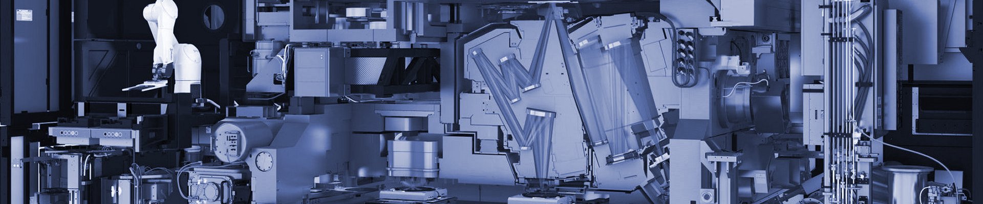
Understanding the ASML EUV scanner requires understanding it as more than a single machine. It is a complete lithography system spanning the scanner itself, the EUV plasma source that produces 13.5 nanometer photons, the reflective optics made exclusively by Carl Zeiss SMT (Germany), the high-power CO₂ laser supplied exclusively by Trumpf (Germany), the vacuum system that must maintain near-perfect conditions across the scanner interior, the reticle and pellicle handling subsystems, the dual-stage wafer handling architecture, the environmental control systems that isolate the scanner from vibration and thermal variation, and a supply chain of several thousand specialty suppliers across Europe, the US, and Japan that together produce the components ASML integrates into each scanner. A single NXE:3800E scanner contains approximately 100,000 individual components and weighs approximately 180 tonnes. The next-generation EXE:5000 High-NA EUV scanner is substantially larger — its primary projection optic mirror alone exceeds one meter in diameter. Production cadence across all generations runs at approximately 40–50 scanners per year globally, a rate that ASML has sustained despite multi-year demand for capacity expansion.
This page covers the ASML EUV scanner as a reference narrative for specialty equipment — who makes it, how it works, what supports it, and what its strategic position looks like. It serves as the template for other narrative equipment pages in the SiliconPlans knowledge graph that cover specific vendor products at specific application tiers (Besi hybrid bonders, Advantest V93000 ATE, FormFactor advanced probe cards, Disco dicing saws, Towa compression molding, Kulicke & Soffa wire bonders, Applied Materials and Lam Research specialty tools).
The Monopoly and Its Origins
ASML's EUV monopoly did not emerge by accident. The company's origin traces to 1984 as a Philips-ASM International joint venture in Veldhoven, Netherlands, focused on semiconductor lithography equipment. For the first two decades, ASML was a distant third in semiconductor lithography behind Nikon and Canon (both Japanese operators with strong incumbent positions). The turning point began in the mid-1990s when ASML committed to EUV as a next-generation lithography path, while Nikon and Canon focused on extending existing optical lithography through immersion and multi-patterning. Through the 1990s and 2000s, ASML and its partners invested approximately $10 billion (across EUV-LLC consortium partners, public research funding, and private investment) to develop EUV technology from research concept to commercial product.
The bet was unprecedented. EUV required entirely new physics — photons at 13.5 nanometer wavelength are absorbed by every material, including air, so the entire scanner must operate in vacuum. Conventional glass optics cannot transmit EUV, so all projection optics must be reflective (mirrors, not lenses). EUV photons cannot be produced by conventional light sources, so a specialty plasma source using vaporized tin droplets was required. The mirror surface finish requirements are more demanding than any optical system ever built — sub-atomic surface roughness across mirror diameters exceeding 30 centimeters. Pellicle protection of EUV reticles presented unsolved problems. Resist chemistry for EUV required new formulations. Every subsystem needed to be developed from first principles because existing optical lithography components did not translate to the EUV regime.
By 2013, ASML had acquired Cymer (the US specialty supplier of EUV plasma sources) for $2.5 billion, consolidating the source subsystem into ASML's organization. By 2015, the first commercial EUV scanner (NXE:3300B) had shipped to TSMC and Samsung for pilot use. By 2018, TSMC began ramping 7nm EUV production using ASML NXE:3400B scanners, marking the commercial transition. Nikon and Canon had effectively withdrawn from the leading-edge race by this point — neither had production EUV capability, and no new entrant was positioned to catch up given the cumulative investment and supply chain requirements. ASML had become a monopoly at the moment EUV became the critical lithography technology for leading-edge logic and memory.
The monopoly is structurally self-reinforcing. ASML's accumulated technical knowledge, its vendor relationships (particularly with Zeiss for optics and Trumpf for lasers), its installed base at major customers, and its ongoing engineering investment together create barriers to entry that no foreseeable competitor can overcome without comparable cumulative investment. The Chinese domestic lithography program at Shanghai Micro Electronics Equipment (SMEE) operates at the 90nm class — roughly 25 years behind EUV capability. Japanese ambitions for EUV capability via Rapidus partnerships do not extend to scanner manufacture. No credible alternative EUV vendor has emerged, and none appears likely to emerge in the 2020s or early 2030s.
How the Scanner Works
An ASML EUV scanner performs lithography — the process that transfers a pattern from a reticle (a master template) onto a photoresist-coated wafer. The specific challenges of EUV lithography at 13.5 nanometer wavelength drive a distinctive system architecture.
Plasma source. The scanner begins with EUV photon generation at the plasma source. A train of approximately 50,000 tin droplets per second — each droplet roughly 25 micrometers in diameter — is generated by a tin droplet generator and directed through the source chamber. A high-power CO₂ laser pulse strikes each droplet as it reaches a specific position, vaporizing the tin into a plasma at temperatures exceeding 220,000 K. This plasma emits EUV photons across a range of wavelengths, but the scanner optics are optimized for the 13.5 nanometer line. The laser-produced plasma (LPP) architecture, developed originally at Cymer and now operated as an ASML subsidiary, was the technology choice that distinguished the successful EUV development path from alternatives that failed to reach commercial scale.
Collector optic. The EUV photons emitted in all directions from the plasma are collected and directed toward the reticle by a specialty collector mirror. The collector must survive the harsh plasma environment (tin contamination, high thermal loads, radiation damage) while reflecting 13.5 nanometer photons with high efficiency. Collector mirror lifetime is a specific operational concern — contamination from the tin plasma gradually degrades the collector, requiring periodic replacement.
Illumination and reticle. The collected EUV light is shaped by illumination optics into the required pupil configuration, then directed onto the reticle. The reticle is a patterned mask made of low-expansion glass coated with a multilayer EUV-reflective surface; specific regions of the reticle have a patterned absorber layer that defines the geometry to be printed. Because EUV cannot pass through conventional pellicles, EUV reticle protection uses specialty thin membrane pellicles developed specifically for EUV — a subsystem with its own supply chain concentrated at Hoya, Mitsui Chemicals, and specialty operators.
Projection optics. The EUV light reflected from the reticle passes through the projection optics — six reflective mirrors manufactured exclusively by Carl Zeiss SMT — that reduce the reticle pattern by 4× and project it onto the wafer. Each mirror must maintain surface figure to sub-atomic precision across mirror diameters up to approximately 30 centimeters for NA=0.33 scanners, or larger for NA=0.55 High-NA scanners. The projection optics are the most demanding optical system ever manufactured at commercial volumes.
Wafer stage and exposure. The wafer sits on a dual-stage architecture that enables continuous throughput: while one wafer is being exposed, the next wafer is being loaded and aligned on the second stage. Wafer stage positioning uses specialty interferometric measurement at sub-nanometer precision. Exposure occurs as the reticle and wafer move in synchronized scan motion, with each die on the wafer exposed sequentially as the reticle pattern steps across.
Vacuum and environmental systems. The entire scanner operates in vacuum because EUV photons are absorbed by any gas. The vacuum system must maintain cleanliness while handling continuous wafer loading and unloading. Environmental isolation includes vibration isolation systems (the scanner sits on active vibration-cancellation platforms), thermal stability (micro-kelvin temperature control), and specialty air handling for the external environment that interfaces with the scanner.
Throughput of a current-generation NXE:3800E scanner is approximately 200 wafers per hour at production conditions. EXE:5000 High-NA EUV scanners are initially operating at lower throughput as the new architecture matures, with throughput scaling toward and beyond the NXE generations as process and tool maturity develops.
Scanner Generations
| Generation | Timeframe | Capability and Applications |
|---|---|---|
| NXE:3100 | 2010–2012 | First pre-production EUV research tool; deployed for customer qualification and process development; low throughput (less than 10 wafers per hour); not used for commercial production |
| NXE:3300B | 2013–2015 | First commercial EUV scanner; deployed at TSMC, Samsung, Intel for pilot line and initial production qualification; throughput approximately 85–125 wafers per hour; essential for initial EUV adoption learning |
| NXE:3350B | 2016–2017 | Productivity improvement generation; throughput approximately 125–150 wafers per hour; first EUV generation deployed for commercial revenue production |
| NXE:3400B / 3400C | 2017–2020 | Primary production workhorse for the first EUV commercial wave; TSMC N7 and N5 ramp; Samsung 7LPP; throughput approximately 135–170 wafers per hour; large installed base |
| NXE:3600D | 2021–2023 | Mainstream production tool for 5nm, 3nm, and early 2nm generations; throughput approximately 160–180 wafers per hour; enhanced dose control and overlay; current majority-volume workhorse across TSMC, Samsung, Intel, memory IDMs |
| NXE:3800E | 2023–2025 ramp | Latest NA=0.33 generation; throughput approximately 195–220 wafers per hour; improved productivity and dose uniformity; deploying at TSMC N2 and similar advanced applications |
| EXE:5000 High-NA | 2024–2026 ramp | New High-NA (0.55) architecture for sub-2nm applications; Intel 18A lead customer; substantially larger optics; initial throughput lower than NXE while architecture matures; long-term throughput targeting parity with and beyond NXE generations |
| EXE:5200 High-NA (planned) | 2026+ projected | Productivity improvement of the High-NA platform; targeting throughput parity with late-generation NXE scanners at High-NA resolution; broad sub-2nm logic deployment |
The generational progression shows two patterns. Within the NA=0.33 generations (NXE:3300B through NXE:3800E), ASML has delivered roughly a 2× throughput improvement from first commercial to latest generation while maintaining resolution at the 13.5 nanometer wavelength limit. Individual scanner capability has improved, but the fundamental resolution has been unchanged — multiple-patterning EUV techniques extend effective resolution beyond single-exposure limits. The transition to NA=0.55 High-NA (EXE:5000 and later) is the resolution step — single-exposure High-NA EUV achieves the resolution that previously required double-patterning at NA=0.33, enabling further node progression toward sub-2nm and 1.4nm applications without multi-patterning complexity.
The Supply Chain Depth
The ASML EUV supply chain is the deepest in semiconductor equipment. ASML integrates components from thousands of suppliers into each scanner, with specific critical subsystems concentrated at a small number of specialty partners. Understanding the supply chain matters because supply chain disruption — whether at ASML itself, at Zeiss optics, at Trumpf lasers, or at specialty Dutch precision engineering firms — propagates directly to scanner production capacity.
Zeiss Semiconductor Manufacturing Technology (SMT). Carl Zeiss SMT (Oberkochen, Germany) is the exclusive supplier of EUV projection optics to ASML. The relationship is structured as a strategic partnership with cross-licensing and joint development. Zeiss SMT operates specialty mirror fabrication facilities where large EUV mirrors are manufactured to sub-atomic surface figure precision. The manufacturing process combines specialty glass substrates (Schott low-expansion glass, Zerodur), specialty polishing processes developed specifically for EUV optics, multilayer reflective coatings applied using specialty deposition tools, and specialty metrology for verification at sub-atomic surface specifications. A single EUV projection optic assembly takes approximately 12 to 18 months to manufacture. Zeiss SMT production capacity is one of the specific bottlenecks on ASML scanner production rate.
Trumpf. Trumpf (Ditzingen, Germany) is the exclusive supplier of high-power CO₂ lasers for EUV plasma sources. Trumpf's specialty CO₂ laser capability — operating at 25 kW or higher continuous power output at the specific wavelengths and pulse characteristics EUV sources require — is the culmination of Trumpf's broader industrial laser business. The Trumpf-ASML relationship predates EUV commercialization by roughly a decade; the two companies developed the specific laser architecture for EUV through sustained joint engineering. Trumpf has no meaningful competition at this specialty laser category. A production CO₂ laser system for EUV has unit pricing in the tens of millions of dollars and delivery lead times of 12 to 18 months from order.
Cymer (wholly owned ASML subsidiary). Cymer (San Diego, California) operated as the independent specialty EUV source supplier until ASML acquired the company in 2013 for approximately $2.5 billion. Now a wholly owned ASML subsidiary, Cymer continues to develop and manufacture the EUV plasma source subsystem at its San Diego facility. The source subsystem — including the droplet generator, the Trumpf laser integration, the collector optic, and the source chamber — is the most complex subsystem on the scanner apart from the Zeiss projection optics. Source lifetime, reliability, and efficiency are specific operational concerns that drive continuous Cymer development.
Dutch precision engineering ecosystem. ASML depends on specialty Dutch precision engineering firms for many sub-assemblies and components. VDL Groep (Eindhoven) operates multiple precision mechanical subsidiaries serving ASML. NTS Group (Eindhoven) produces precision mechanical assemblies including wafer and reticle handling subsystems. Prodrive Technologies (Son) provides specialty electronics and control systems. ASM Pacific Dutch operations and specialty firms including Demcon, Settels Savenije, and TNO Technical Sciences together form a Dutch precision engineering cluster in the southeastern Netherlands that has grown with ASML's demand. This cluster is regionally concentrated in the Brabant region around Eindhoven, making it geographically specific and difficult to relocate.
Specialty optical and vacuum components. Specialty suppliers including Schott (specialty glass for optics substrates), Integrated Dynamics Engineering (vibration isolation), Newport Corporation (specialty optomechanics), Janis Research and specialty cryogenic operators (specialty thermal control), and numerous others serve specific subsystem requirements. Japanese specialty suppliers including Mitutoyo (specialty metrology), Nikon and Canon (specialty optics subsidiaries serving ASML for non-competing subsystems), and specialty Japanese precision engineering firms provide additional components.
EUV mask and pellicle ecosystem. Although not directly part of the scanner supply chain, the EUV mask ecosystem is essential for scanner utilization. Hoya (Japan) dominates EUV mask blank production. Lasertec (Japan) dominates actinic EUV mask inspection (specialty tool separate from KLA's broader inspection business). Mitsui Chemicals and specialty operators produce EUV pellicles. The mask and pellicle supply chain concentrations are each specific single-vendor or oligopolistic structures that parallel ASML's scanner monopoly at their specialty level.
The Customer Install Base
ASML EUV scanners are deployed at a specific set of leading-edge semiconductor operators. The installed base is well-documented because EUV scanner sales are large enough that each installation is publicly announced or verifiable.
TSMC operates the largest EUV installed base globally. TSMC has deployed EUV scanners across multiple generations (NXE:3300B through NXE:3800E) for its 7nm, 5nm, 3nm, and 2nm logic production. The cumulative TSMC EUV installed base is estimated at 100+ scanners across Fab 12, Fab 14, Fab 18, and Fab 21 (the US Arizona fab), with TSMC Japan JASM adding further EUV capacity. TSMC's EUV deployment timeline has consistently led industry adoption — from initial 7nm EUV pilot through current N2 ramp and planned High-NA EUV adoption.
Samsung Foundry and Samsung Memory. Samsung operates the second-largest EUV installed base, split between Samsung Foundry's logic operations at Hwaseong and Pyeongtaek (advanced logic nodes 7LPP through 3GAE/2GAP) and Samsung Memory's DRAM operations at Pyeongtaek and Hwaseong (HBM-generation and advanced commodity DRAM). Samsung has deployed all major EUV generations and is an early High-NA EUV customer.
Intel has been expanding its EUV install base substantially as Intel 18A and later nodes ramp. Intel is the lead High-NA EUV customer — Intel's Fab 52 Arizona deployment and Oregon D1X Mod 3 operations are the first commercial EXE:5000 High-NA EUV deployments globally. Intel's transition from zero EUV (initial Intel 7 generations used no EUV) to substantial EUV install base represents Intel's broader manufacturing modernization under Pat Gelsinger's leadership.
SK hynix and Samsung Memory for HBM. EUV is increasingly deployed at DRAM production for HBM3e, HBM4, and advanced commodity DRAM D1x and D1y nodes. SK hynix EUV installations at Icheon and specific advanced DRAM lines, Samsung Memory EUV, and Micron's selective EUV adoption together constitute a meaningful EUV memory installed base.
Micron has been later to EUV adoption than Samsung or SK hynix but has deployed EUV selectively at its leading DRAM lines.
Rapidus (Japan) has ordered EUV scanners for its planned 2nm Japanese fab ramp. Rapidus ordered a complete EUV toolset including NXE:3800E generation scanners and eventual High-NA EUV integration — the first major Japanese deployment of EUV at scale in a decade.
No Chinese customer. Chinese semiconductor operators including SMIC, YMTC, CXMT, and others have no EUV scanners and cannot acquire them under current export control restrictions. This is the specific most-visible manifestation of US and allied semiconductor export controls — Chinese leading-edge logic and advanced memory advancement is constrained specifically by the inability to access EUV. See below for the export control framework.
Economics and Production Cadence
ASML EUV scanner economics are distinctive in semiconductor equipment. Per-scanner pricing for NA=0.33 generation NXE scanners runs approximately $180 to $220 million depending on configuration and generation. EXE:5000 High-NA EUV pricing runs approximately $350 to $400+ million per scanner. Including support infrastructure (vacuum systems, air handling, specialty facility requirements, installation, initial qualification) each scanner deployment represents capital expenditure of $250 million or more at NA=0.33 and $450 million or more at High-NA.
ASML's EUV revenue has been approximately €15–20 billion annually in recent years with continuing growth. Production cadence is approximately 40 to 50 NXE scanners per year at current production rates, with High-NA EUV ramping alongside. The production cadence is the specific capacity constraint on industry-wide leading-edge capacity expansion — TSMC, Samsung, Intel, and the memory IDMs collectively demand more EUV scanners than ASML can produce, with allocation decisions that affect customer capacity planning. ASML has invested in expanding production capacity at Veldhoven and through supply chain partner capacity expansions.
Lead times from order to scanner installation run 18 to 24 months at current demand levels. This means capacity for 2027 production must be ordered in late 2025 or early 2026; capacity for 2028 in 2026 or 2027. The multi-year planning horizon creates substantial coordination burden for customers making capital commitment decisions — fab construction, EUV order, and downstream customer demand must all align on timescales years in advance.
Operational economics favor extreme utilization. An EUV scanner operating at 200 wafers per hour across 22 hours per day produces approximately 1.6 million wafer exposures per year. Capital amortization over a 10-year scanner lifetime produces per-wafer amortization cost of approximately $12 to $20 depending on specific utilization and pricing assumptions. Customer economics justify EUV investment because the wafer value at leading-edge nodes (N5, N3, N2) is substantial — the per-wafer EUV amortization is a relatively small fraction of total wafer cost at leading-edge logic.
Export Controls and Geopolitics
ASML EUV scanners are the specific most-prominent target of US-led semiconductor export controls affecting China. The control framework has evolved over approximately six years and continues to tighten.
The structural framework involves coordination between US Bureau of Industry and Security (BIS), the Netherlands government (where ASML is headquartered and manufacturing is concentrated), and allied governments. The Netherlands applies export controls on ASML EUV scanners; the US applies extraterritorial controls on US-origin components (primarily Cymer EUV source subsystem and specialty US-supplied components). Together these controls have effectively prevented EUV scanner shipments to China for all practical purposes since approximately 2019.
No EUV scanner has been exported to a Chinese customer. Chinese operators including SMIC, YMTC, CXMT, and Huawei-adjacent operators have no EUV capability and have no path to acquiring EUV under current restrictions. This is the specific technological gap that prevents Chinese leading-edge logic and advanced memory from reaching parity with TSMC, Samsung, Intel, and the Western memory IDMs. Chinese domestic EUV development at Shanghai Micro Electronics Equipment (SMEE) operates approximately 25 years behind commercial EUV capability and is not projected to close the gap in the foreseeable future.
DUV controls are tiered. ASML DUV scanners (deep ultraviolet, 193 nanometer wavelength, used for mature nodes) face less stringent but still meaningful controls. Advanced DUV immersion scanners used for leading mature nodes and some 7nm production are increasingly controlled, while older DUV dry scanners remain more accessible. The tiered control approach reflects the strategic distinction between EUV (flagship leading-edge, no alternative) and DUV (multiple vendors historically, still essential for mature production).
2024 restrictions tightened EUV-adjacent controls further, particularly around service, maintenance, and upgrade activities for ASML scanners at customers in restricted jurisdictions. Some controls have been framed as preventive against technology leakage rather than preventing new sales (since new sales were already prohibited).
The export control regime has broader structural implications. It defines the specific technology gap between Chinese domestic leading-edge capability and Western leading-edge capability. It creates strategic dependencies between the Netherlands government and US policy coordination — ASML is structurally valuable to Dutch policy as a sovereign-capable technology company but dependent on US component supply that the Netherlands cannot unilaterally insulate. The gap between TSMC, Samsung, and Intel at advanced nodes (enabled by EUV) and Chinese domestic alternatives (constrained to 7nm-class using multi-patterned DUV at SMIC N+1 and N+2) is the specific technology differential that US policy aims to sustain.
The High-NA EUV Transition
ASML's EXE:5000 High-NA EUV represents the next generation of EUV lithography and is the specific scanner that will drive sub-2nm leading-edge logic adoption. The High-NA architecture differs from NA=0.33 EUV in several fundamental ways.
Higher numerical aperture. NA=0.55 optics provide approximately 1.7× better resolution than NA=0.33 at the same wavelength (13.5 nanometer). This means single-exposure High-NA EUV achieves resolution that previously required double-patterning at NA=0.33 — enabling simpler process flows for advanced nodes.
Larger optics. The High-NA projection optics use substantially larger mirrors than NA=0.33 optics. The largest mirror in the EXE:5000 optics exceeds one meter in diameter — a manufacturing challenge that Zeiss SMT has addressed through specialty new fabrication capabilities. The larger optics drive higher per-scanner cost and more specialty supply chain requirements.
Half-field exposure. High-NA EUV scanners expose a half-field at the wafer (approximately 26 × 16.5 mm) versus the full field (approximately 26 × 33 mm) of NA=0.33 scanners. This halves the exposed area per exposure shot, which has implications for die size and cost — dies larger than the High-NA half-field require field stitching. Engineering design rules and process adaptations accommodate this constraint.
New resist and mask requirements. High-NA EUV resist chemistry and mask technology face specific requirements at the higher NA. Specialty resist development and mask inspection tools at High-NA generation are downstream capabilities that must be developed alongside the scanner.
Intel as lead customer. Intel's Arizona Fab 52 deployment of EXE:5000 is the first commercial High-NA EUV installation. Intel's specific choice of leading High-NA adoption reflects Intel's strategy of manufacturing leadership — being the first to deploy High-NA creates a window of advantage against TSMC (which has signaled that it will adopt High-NA at a slightly later cadence) and Samsung. The High-NA learning at Intel will likely precede broader industry adoption.
High-NA EUV ramp will occur through the late 2020s. Industry expectation is that High-NA becomes the mainstream leading-edge lithography by approximately 2027–2029, with NA=0.33 remaining in mainstream use for mature EUV applications (7nm, 5nm, 3nm class generations that will remain in high-volume production for many years) and for specific applications where High-NA's half-field limitation would require fab redesign.
Operational and Maintenance Considerations
ASML EUV scanner operational economics require substantial ongoing support infrastructure. Each scanner has associated service teams (ASML field engineers plus customer operational staff) providing continuous preventive and corrective maintenance. Routine maintenance includes tin source cleaning and replacement (collector mirror refurbishment or replacement every 6–12 months depending on utilization), vacuum system servicing, optics cleaning, and specialty calibration activities. Each scanner operates with associated consumables, spare parts inventory, and specialty operational supplies.
Scanner uptime metrics are closely tracked. Industry expectation for mature-generation EUV scanners is greater than 90% availability at high utilization; advanced generations ramp from lower initial availability to mature rates over the first 1–2 years of deployment. Downtime from tin source issues, vacuum excursions, optics contamination, or specialty subsystem failures directly affects production throughput and is treated as a specific operational priority.
Tool upgrade paths exist within generations. Specific incremental capability additions (dose control improvements, overlay enhancement, specialty metrology integration) are delivered via upgrade packages that customers apply to existing scanners. Cross-generation upgrades (NXE to EXE transition) are not feasible — High-NA architecture is sufficiently different that it requires new scanner installation rather than upgrade.
Strategic Positioning
The ASML EUV scanner occupies a structural position without close parallel in semiconductor equipment or in broader technology industries. Single-supplier monopoly positions in high-end equipment are rare globally; ASML's position is the most extreme case of such concentration for a product category of comparable strategic importance. The closest structural analogs are specialty aerospace propulsion (where specific high-end jet engine components concentrate at narrow vendor bases), specialty scientific instrumentation (where specialty particle accelerators or specialty electron microscopes concentrate at single suppliers), and specialty military systems where single-supplier dependencies are common but at smaller commercial scale.
The structural significance of the ASML monopoly propagates through the industry in multiple ways. Customer concentration risk — TSMC, Samsung, Intel, and the memory IDMs are all dependent on ASML for EUV access, with no alternative supplier to hedge against ASML disruption. Geopolitical leverage — US and Netherlands policy coordination on ASML exports has become a specific instrument of Western technology policy against Chinese semiconductor advancement. Capacity allocation — ASML allocation decisions among customers affect customer leading-edge capacity plans. Supply chain propagation — Zeiss, Trumpf, and the specialty supplier base for ASML are each specialty dependencies that cascade back from ASML's position to their own positions.
The ASML position is unlikely to change structurally within the current decade. The barriers to entry — accumulated investment, specialty supply chain, customer operational dependencies, ongoing technology advancement — are too substantial for a new entrant to bridge on short timescales. The most likely scenarios are continued ASML monopoly through at least the mid-2030s, with incremental technology evolution (High-NA generational progression, potential next-generation wavelength or architecture work at ASML R&D) maintaining the structural position.
Related Coverage
Parent categories: Wafer Fab Equipment · Lithography
Related WFE narrative pages (planned): ASML DUV immersion scanners · ASML High-NA EUV specialty · Nikon and Canon legacy lithography
EUV ecosystem dependencies: Zeiss SMT (EUV optics) · Trumpf (CO₂ laser) · Cymer (EUV source, ASML subsidiary) · Hoya (EUV mask blanks) · Lasertec (actinic EUV mask inspection) · Mitsui Chemicals and specialty (EUV pellicles)
Customer-side coverage: Leading-Edge Logic Fabs · DRAM Fabs (EUV HBM applications)
Export controls framing: U.S. Reshoring · Export Controls & Chinese Semiconductor Advancement (planned strategic framing page)
Strategic framing: Bottleneck Atlas (EUV as primary capacity chokepoint for leading-edge logic and HBM-class DRAM)
Vendor profile (planned): ASML Holding