SemiconductorX > Fab & Assembly > Wafer Fab Equipment > Lithography
WFE Lithography Equipment
Lithography equipment is the most concentrated category in wafer fab equipment — and the most strategically consequential. ASML supplies every EUV and High-NA EUV scanner manufactured on earth, approximately 85–90% of DUV immersion scanners for leading-edge production, and holds the technology pipeline for every generation beyond. Nikon and Canon supply the remaining DUV market at mature nodes and for specialty applications. SMEE (Shanghai Micro Electronics Equipment) is China's domestic lithography champion and serves the Chinese market at DUV dry and early-immersion tiers. No other credible vendor operates at meaningful scale.
This page covers the lithography layer of the fab through the equipment and vendor lens — tool classes, vendor market positions, tool family taxonomies, the supporting ecosystem (mask writers, pellicles, coater-developers), and the installation logistics specific to lithography scanners. For the process-activity view — what lithography does physically on the wafer, how resolution works, photoresist chemistry — see Photolithography (process lens).
The Three Tool Classes
Commercial lithography scanners divide into three classes by light source and optical system. Each class serves a specific node range and carries its own cost, lead-time, and export-control profile.
| Tool Class | Wavelength & Optics | Node Applicability | Cost per Tool |
|---|---|---|---|
| DUV Dry | 248 nm (KrF) or 193 nm (ArF); conventional air-gap optics | 180 nm and above mature nodes; legacy production; specialty analog and power | $15–30M per scanner |
| DUV Immersion | 193 nm (ArF) with water immersion between lens and wafer; effective ~38 nm half-pitch | 28 nm down to 7 nm with multipatterning; workhorse of mature-advanced production globally; SMIC N+1 path | $50–80M per scanner |
| EUV (0.33 NA) | 13.5 nm from laser-produced tin plasma; reflective Mo-Si multilayer optics in vacuum | Mandatory at 7 nm and below for competitive production; TSMC N5/N3/N2, Samsung SF4/SF3/SF2, Intel 4/3/18A | $150–200M per scanner |
| High-NA EUV (0.55 NA) | 13.5 nm; higher numerical aperture optics; anamorphic magnification; vacuum system | Sub-2 nm nodes: Intel 14A, TSMC A14, Samsung SF2 and successors | ~$380M per scanner |
The cost gap between DUV and EUV is roughly 3–4×; the gap from EUV to High-NA EUV is roughly 2×. A leading-edge fab with full EUV deployment requires 15–25 EUV scanners plus multiple DUV immersion scanners for non-critical layers — an equipment investment measured in several billion dollars for the scanner set alone, before deposition, etch, and metrology tools are added.
Vendor Landscape
The lithography scanner market has narrowed progressively over four decades. Perkin-Elmer, GCA, Ultratech, and a half-dozen other vendors have exited since the 1990s. The current market structure is one dominant player (ASML), two secondary DUV vendors (Nikon, Canon), and one Chinese domestic challenger at DUV tiers (SMEE). No new entrant is expected at the EUV tier within this decade given the development timelines and capital required.
| Vendor (HQ) | Tool Families | Market Position & Customers |
|---|---|---|
| ASML (Veldhoven, Netherlands) | Twinscan NXT (DUV immersion); Twinscan NXE (EUV 0.33 NA); Twinscan EXE:5000 (High-NA EUV 0.55 NA); YieldStar metrology and stepper variants | Sole EUV and High-NA EUV supplier globally; ~85–90% of DUV immersion market; every leading-edge foundry customer including TSMC, Samsung, Intel, Micron, SK hynix |
| Nikon (Tokyo, Japan) | NSR-S series DUV immersion (S620D, S621D, S622D); NSR-S635E DUV for mature nodes; NSR-S650E specialty | Secondary DUV vendor; historical Intel partnership; mature-node immersion capacity; packaging lithography; exited EUV development after decade-plus R&D investment |
| Canon (Tokyo, Japan) | FPA-6300/FPA-5550 i-line and KrF steppers; packaging lithography; FPA-1200NZ2C nanoimprint lithography (emerging) | Mature-node DUV dry and i-line; advanced packaging lithography; nanoimprint lithography as differentiated roadmap bet (Kioxia 3D NAND customer); exited EUV development |
| SMEE (Shanghai, China) | SSA/800 series DUV dry (production); early DUV immersion in development (SSA/900 reported) | China domestic DUV dry supplier; 90 nm production-qualified; 28 nm development reported; strategic Chinese push to replace ASML/Nikon at mature nodes; no credible near-term EUV path |
| EV Group (Sankt Florian, Austria) | Specialty lithography for compound semiconductor, MEMS, advanced packaging; imprint and bond-align systems | Specialty applications outside mainstream logic; complements mainstream scanners rather than competing |
| SÜSS MicroTec (Garching, Germany) | Specialty lithography and photomask equipment; MEMS and LED lithography; advanced packaging steppers | MEMS, LED, advanced packaging specialty; non-competing with mainstream IC lithography |
The two Japanese vendors (Nikon, Canon) both attempted EUV development and both exited the EUV race. The capital, supply chain, and optical-system development required for EUV proved uneconomic for vendors without ASML's scale and without the Intel/Samsung/TSMC equity-investment backing that funded ASML's EUV development. Canon has pivoted toward nanoimprint lithography as a differentiated path — a non-optical patterning technique with cost advantages at specific applications (3D NAND, some specialty markets) — but nanoimprint is not a near-term threat to EUV at leading-edge logic. SMEE's DUV domestic track serves Chinese domestic demand at mature nodes and is expanding under government support; Chinese progress beyond DUV immersion is gated by foreign optical system dependencies that remain difficult to replace domestically.
The ASML Tool Family Taxonomy
ASML's lithography product line is structured across three families: NXT (DUV immersion), NXE (EUV), and EXE (High-NA EUV). Each family has successive generations with incremental throughput, overlay, and resolution improvements.
| Platform | Latest Generation | Position |
|---|---|---|
| Twinscan NXT (DUV Immersion) | NXT:2100i, NXT:2050i, NXT:2000i, NXT:1980Di generations | Workhorse DUV immersion platform; critical for non-EUV layers at all leading nodes plus mainstream 7/10/28 nm production; highest-volume ASML product by unit count |
| Twinscan NXE (EUV 0.33 NA) | NXE:3800E, NXE:3600D, NXE:3400 series | Sole EUV platform globally; production rate ~40–55 units per year; 18–24 month lead time from order to install; $150–200M per tool |
| Twinscan EXE (High-NA EUV 0.55 NA) | EXE:5000 (first production unit at Intel, 2024) | Sole High-NA EUV platform; ~20 units in 2025 ramping toward 30+ by 2027; ~$380M per tool; Intel launch customer; TSMC and Samsung ordered |
| Twinscan XT (DUV Dry) | XT:1460K, XT:1060, legacy dry platforms | Mature-node DUV dry for nodes above immersion necessity; specialty applications |
| YieldStar | YieldStar 1385, YieldStar 375 | Overlay and CD metrology that pairs with scanner fleet; integrates with KLA process control |
ASML's NXT immersion platform is often overlooked in geopolitical discussion because EUV dominates the narrative, but NXT is the volume workhorse of global leading-edge production: even an all-EUV fab runs more DUV immersion layers than EUV layers per wafer. Any disruption to NXT production would affect production across essentially every foundry worldwide, not just the foundries that have EUV. Dutch export controls on NXT:2000i-class tools to China (tightened in 2023 and extended in subsequent rules) reflect this strategic reality.
The Supporting Lithography Ecosystem
Lithography scanners do not operate alone. Each lithography bay at a modern fab combines the scanner with a matched set of supporting tools, consumables, and service equipment. The support ecosystem is its own concentrated supply story.
| Ecosystem Element | Role | Vendor Concentration |
|---|---|---|
| Coater-Developer (Track) Systems | Apply photoresist before exposure; develop after exposure; integrate directly with scanner in the lithography cluster | Tokyo Electron (TEL) dominant globally at >85% market share; SCREEN secondary; without TEL track capacity, scanner capacity cannot be used |
| Photomask Writing (E-Beam) | Fabricate the reticles that contain the circuit pattern to be projected onto the wafer; multi-beam e-beam writers for advanced masks | NuFlare Technology (Toshiba subsidiary); JEOL; IMS Nanofabrication (Intel-owned); Advantest acquired ADT mask metrology |
| Photomask Inspection | Verify mask quality before mask ships to fab; EUV masks require specialized actinic inspection at 13.5 nm | KLA (mask inspection systems); Lasertec (actinic EUV mask inspection — sole global supplier of EUV-wavelength mask inspection); Hitachi High-Tech secondary |
| Pellicles | Thin protective membrane above the reticle that prevents particles from falling onto the pattern surface during exposure; EUV pellicles operate at 13.5 nm in vacuum | Mitsui Chemicals; Asahi Kasei; Shin-Etsu; Canon Tokki (EUV pellicle specialty); EUV pellicle supply has been capacity-constrained |
| Photomask Blanks (Substrates) | Ultra-flat quartz substrates with chrome or metal absorber layers; the physical substrate on which circuit patterns are written | Hoya (dominant globally, especially for EUV blanks); SK hynix SK Enmos for mask substrates; Shin-Etsu |
| Photoresist | Photosensitive polymer that receives the pattern from scanner exposure; EUV requires specialty resist formulations | JSR, Tokyo Ohka Kogyo (TOK), Shin-Etsu, Fujifilm, Sumitomo Chemical; EUV resist dominated by Japanese specialty suppliers |
The TEL coater-developer concentration is the most operationally important supporting-ecosystem fact in lithography: TEL holds an effective monopoly on the track systems that integrate with ASML scanners, and scanner productivity is bottlenecked by track throughput. Fabs cannot increase lithography throughput by buying more scanners without matching TEL track capacity. This coupling — ASML scanner plus TEL track — is a de facto duopoly controlling the throughput of every lithography bay at every leading-edge fab globally.
The Lasertec actinic EUV mask inspection position is another overlooked monopoly: Lasertec is the sole global supplier of EUV-wavelength actinic mask inspection systems, without which EUV masks cannot be reliably qualified before use. The combination of Hoya (EUV mask blanks), Lasertec (EUV mask inspection), and ASML (EUV scanners) describes the trio of single-point concentrations that gate EUV production.
Lead Times & Installation
Lithography scanners have the longest lead times in wafer fab equipment. An ASML EUV scanner runs 18–24 months from order to installed and qualified tool. High-NA EUV runs longer still, reflecting supply chain ramp. DUV immersion runs 12–18 months. DUV dry runs 9–15 months. These lead times are structural — they reflect manufacturing complexity, test cycles, and supply-chain ramp at Carl Zeiss SMT, Trumpf, and Cymer — not inventory policy. Fabs announced under CHIPS Act and EU Chips Act programs that require EUV scanners are working against this lead-time reality for every tool in their configuration.
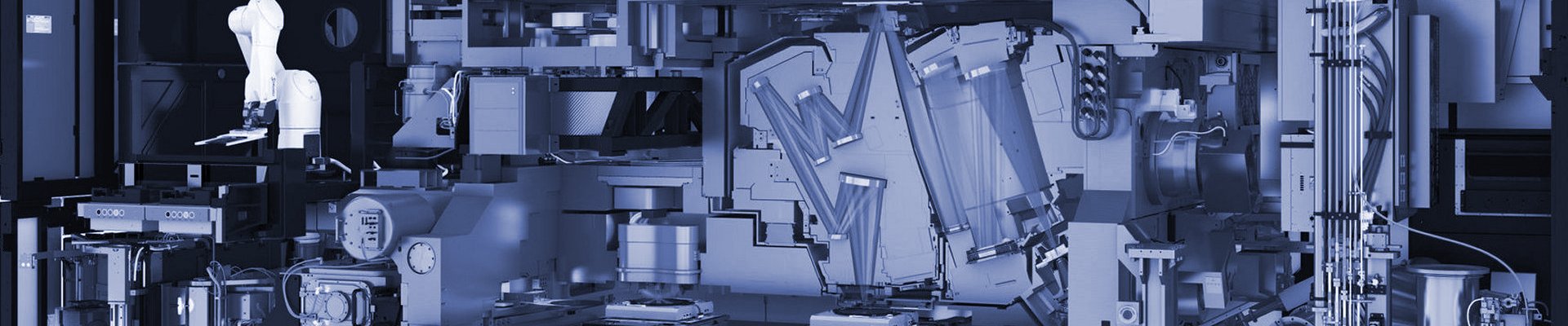
Installation logistics at the fab are equally demanding. EUV scanners ship in multiple crates totaling approximately 165 tons of equipment, move via specialized Boeing 747 freighters and custom ground transport, and require months of on-site assembly and calibration. Fab floors must be prepared with vibration-isolated foundations, electromagnetic shielding, hydrogen and ultrapure water supply, specialized power delivery, and the cleanroom conditions required for a machine that operates at 13.5 nm wavelength in hard vacuum. Installation of a single EUV scanner is a major civil engineering project in itself.
Export Controls Specific to Lithography
Lithography export controls are the most restrictive in the WFE sector and the most politically active. EUV tools have been blocked from China since 2019 by the Netherlands government, with tightening coordinated between the Netherlands, United States, and Japan through the Wassenaar Arrangement framework. Advanced DUV immersion tools (ASML NXT:2000i and above) have been restricted since 2023, closing the upstream of the multipatterning path that had allowed SMIC's N+1 7 nm-equivalent production. Nikon advanced immersion tools and Canon specialty tools fall under Japanese 2023 export controls. SMEE's Chinese domestic DUV tools are the intended substitute pathway but face technology gaps at the immersion tier.
The practical effect is a bifurcated lithography market: Western-and-allied foundries access the full ASML, Nikon, Canon supply with coordinated licensing; Chinese foundries are progressively restricted from the leading-edge tool set and must rely on a combination of pre-restriction DUV installed base plus SMEE domestic production for future capacity. This gap compounds with every new lithography generation.
Related Coverage
Parent: Wafer Fab Equipment
Process-activity lens: Photolithography (same step, physics/process view)