SemiconductorX > Fab & Assembly > Wafer Fab Equipment > Cleaning
WFE Cleaning Equipment
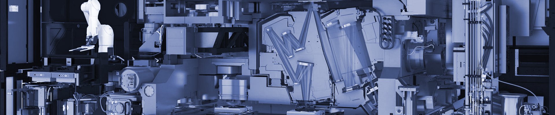
Cleaning equipment is the highest-cycle category in wafer fab equipment — a wafer may pass through 50 to 100+ cleaning steps across the full production flow, making cleaning throughput a primary gate on overall fab throughput. The vendor landscape is more concentrated than deposition or etch. SCREEN Holdings (Japan) holds dominant global position, particularly in single-wafer wet cleaning where SCREEN's share exceeds 50% in key categories. Tokyo Electron is the strong secondary vendor with strength in batch cleaning and specialty single-wafer applications. SEMES (South Korea, Samsung subsidiary) operates a distinctive captive-plus-external model — supplying Samsung Foundry and Samsung Memory captively plus limited external customers. Lam Research and Applied Materials operate smaller positions in specialty applications.
This page covers cleaning through the equipment and vendor lens — tool architectures, vendor market positions, tool family taxonomies, and the specialty cleaning chemistry supply that the equipment consumes. For the process-activity view — what cleaning does physically on the wafer, surface chemistry, SC1 and SC2 principles, particle removal mechanisms — see Cleaning (process lens).
Two Architectural Splits
Cleaning equipment is segmented along two orthogonal architectural dimensions. The first split is by cleaning modality — wet versus dry. The second split is by wafer handling — batch versus single-wafer. Together these produce four distinct tool categories, each with its own vendor mix and application range.
| Tool Category | Architecture | Primary Applications |
|---|---|---|
| Single-Wafer Wet Clean | One wafer processed at a time with precise chemistry dispense, rinse, and dry; programmable chemistry sequences | Critical layers at advanced nodes; post-etch residue removal; pre-deposition surface preparation; advanced-node clean steps requiring chemistry precision |
| Batch Wet Clean | Multiple wafers (25–50) processed simultaneously in chemistry baths; higher throughput per tool | Non-critical bulk cleaning; blanket oxide strip; pre-thermal-processing clean; mature-node applications where single-wafer precision not required |
| Dry Plasma Clean | Plasma-based removal of residues and organics; typically integrated with etch or deposition tools or as standalone dry clean stations | Photoresist ash and strip; organic residue removal; in-situ chamber clean between etch or deposition steps; post-implant residue removal |
| Supercritical CO₂ (sCO₂) Drying | Post-clean drying using supercritical CO₂ to avoid capillary forces that cause pattern collapse in high-aspect-ratio structures | High-aspect-ratio drying at FinFET fins, GAA nanosheets, 3D NAND channel holes, DRAM capacitor trenches; essential at advanced nodes where conventional drying collapses patterns |
The single-wafer wet clean category is where SCREEN's dominance is most pronounced and where the industry growth has concentrated. Batch wet clean remains significant at mature nodes but is displaced by single-wafer architectures at leading nodes because the chemistry precision required at sub-7 nm cannot be achieved in a shared bath. Supercritical CO₂ drying, a technology once considered exotic, has become essential at advanced nodes where conventional water-based drying causes pattern collapse in high-aspect-ratio structures — SCREEN's specialty position in this category has been a key driver of its overall dominance.
The Pattern Collapse Problem and sCO₂ Drying
High-aspect-ratio structures — FinFET fins with aspect ratios of 5:1, GAA nanosheet stacks at 10:1, 3D NAND channel holes at 100:1 — face a counterintuitive physics problem during drying. When a wet structure dries via conventional evaporation, surface tension at the water-air interface pulls adjacent structures together. At high aspect ratios, this capillary force exceeds the structural rigidity of the feature and causes the structures to collapse against each other, destroying the patterning. A FinFET fin that withstood etch and cleaning will collapse during the drying step if not dried properly.
Supercritical CO₂ drying solves this by raising CO₂ above its critical point (31°C, 74 bar) where the liquid-gas phase boundary disappears entirely, allowing drying without surface tension. The wafer is transitioned from wet chemistry through an IPA (isopropanol) rinse to liquid CO₂ to supercritical CO₂ to gaseous CO₂, all without crossing a phase boundary that would create capillary forces. The process is expensive in equipment and consumables but becomes non-negotiable at aspect ratios above approximately 20:1.
SCREEN's sCO₂ drying systems are the reference platforms in this category. TEL and specialty vendors have parallel capability but SCREEN's combination of sCO₂ expertise with its broader single-wafer wet clean dominance positions the company as effectively the reference vendor for advanced-node cleaning. Every new 3D NAND generation, every new GAA node, and every advanced HBM generation increases the demand for sCO₂ drying capacity — which translates directly to SCREEN demand.
Vendor Landscape
| Vendor (HQ) | Primary Cleaning Positions | Market Position |
|---|---|---|
| SCREEN Holdings (Kyoto, Japan) | Single-wafer wet clean (dominant); sCO₂ drying (reference platform); batch wet clean; specialty cleaning | >50% single-wafer wet clean share; reference platform for advanced-node cleaning; SU-3000 and SU-3100 flagship platforms; global customer base including TSMC, Samsung, Intel, Micron, SK hynix |
| Tokyo Electron / TEL (Tokyo, Japan) | Batch wet clean; single-wafer wet clean (secondary to SCREEN); specialty single-wafer applications | Strong secondary in cleaning globally; CELLESTA and Telius Clean platforms; strong at Japanese memory customers; batch cleaning market leader for mature nodes |
| SEMES (Cheonan, South Korea) | Single-wafer wet clean; batch wet clean; specialty cleaning for Samsung operations | Samsung Group subsidiary; primary supplier to Samsung Foundry and Samsung Memory captive; limited external customer business; captive-plus-external model distinctive in WFE |
| Lam Research (Fremont, CA) | Single-wafer wet clean for specialty applications; dry plasma clean integrated with etch platforms; specialty applications | Smaller position in standalone cleaning; integrated clean capability within etch flow; specialty advanced-node applications |
| Applied Materials (Santa Clara, CA) | Dry plasma clean; specialty clean applications; integrated clean with deposition and etch | Smaller position in standalone cleaning; integrated clean capability within broader platforms |
| ACM Research (Fremont, CA / Shanghai) | Single-wafer wet clean; specialty SAPS (space alternated phase shift) and TEBO (timely energized bubble oscillation) cleaning technologies | Dual US-China operational model with Shanghai operations serving Chinese market; specialty single-wafer wet clean platforms with distinctive technology approaches; significant Chinese customer position including SMIC and Yangtze Memory |
The SEMES Captive-Plus-External Model
SEMES is structurally distinctive in WFE as a captive-plus-external equipment vendor. The company is a Samsung Group subsidiary whose primary role is supplying cleaning (and other specialty equipment) to Samsung Foundry and Samsung Memory operations. SEMES effectively functions as an internal Samsung WFE supplier, ensuring Samsung has supply continuity and cost advantage for cleaning equipment without full dependency on external vendors. The external customer business is secondary and selective.
This model has parallels in other parts of the Samsung ecosystem — Samsung Electro-Mechanics for passives and substrates, various Samsung specialty suppliers — but SEMES's position in cleaning makes it particularly strategic. Samsung's cleaning requirements are substantial given the company's fab footprint, and SEMES's captive role means Samsung's cleaning equipment CapEx flows back into the Samsung Group rather than to external vendors. From a supply chain mapping perspective, SEMES is effectively a Samsung-internal capability expressed in corporate form as a subsidiary supplier.
The limited external customer position means SEMES is less visible in global WFE coverage than its production scale would suggest. Its installed base is predominantly captive; its external business is a small fraction of its output. Understanding SEMES is part of understanding how captive WFE supply works at the integrated foundries that operate them (Samsung's SEMES; some Intel internal capability; TSMC's more limited captive manufacturing).
ACM Research and the China Single-Wafer Position
ACM Research is a structurally interesting company in the cleaning vendor landscape. ACM operates a dual US-China model — US headquarters in Fremont, California, with substantial R&D and production operations in Shanghai — and has developed distinctive single-wafer wet clean technologies (SAPS ultrasonic cleaning, TEBO bubble-based cleaning) that differentiate it from SCREEN's and TEL's approaches. ACM has achieved meaningful customer adoption at Chinese fabs including SMIC and Yangtze Memory (YMTC) and has also secured some Korean customer positions.
The ACM position matters for the Chinese WFE substitution story. Unlike the Chinese WFE companies that have faced capability gaps at advanced nodes, ACM has developed genuinely distinctive cleaning technology that has achieved qualification at non-Chinese foundries. The company's dual-geography structure has navigated complex export control environments, and its Shanghai operations position it to serve Chinese customers even as US-China equipment trade has become more restricted. ACM is not a substitute for SCREEN at leading-edge Western foundries, but it is a credible non-Japanese cleaning vendor with distinctive technology — which is a rarity in the broader Chinese WFE substitution effort.
Cleaning Chemistry Supply
Cleaning equipment consumes very large volumes of specialty chemicals — the ultrapure acids, bases, and oxidizers that perform the actual cleaning. Unlike deposition precursors or etch gases where concentration is in a handful of specialty suppliers, cleaning chemistry supply has a broader vendor base but still exhibits supply chain concentration at the purity levels required for advanced nodes.
| Chemistry Category | Primary Suppliers | Application |
|---|---|---|
| SC1 / APM (ammonia-hydrogen peroxide) | Kanto Chemical; Stella Chemifa; Mitsubishi Chemical; KMG; BASF | Particle removal and slight silicon etch; standard post-process clean at every node |
| SC2 / HPM (hydrochloric acid-hydrogen peroxide) | Kanto Chemical; Stella Chemifa; Mitsubishi Chemical; BASF | Metallic contamination removal; standard follow-up to SC1 |
| Hydrofluoric Acid (HF) | Stella Chemifa (Japan, dominant); Solvay; Daikin; Morita Chemical | Native oxide removal; selective etch; pre-gate clean; Japanese supply concentration tightly intertwined with Japan-Korea specialty chemistry trade |
| Sulfuric Acid / Hydrogen Peroxide (SPM / Piranha) | BASF; Kanto Chemical; Mitsubishi Chemical; Chemtrade | Aggressive organic removal; photoresist stripping; heavy residue clean |
| Ozonated DI Water (O₃/DIW) | Generated on-site at fabs using ozone generators; MKS Instruments, Mitsubishi Electric ozone generation systems | Post-etch residue removal; specialty cleaning; low-temperature alternative to SPM for organics |
| CO₂ (for sCO₂ Drying) | Air Liquide; Linde; Taiyo Nippon Sanso; local industrial gas suppliers | Supercritical CO₂ drying consumables; purity requirements are high but supply broader than specialty gases |
The 2019 Japan-Korea trade friction specifically named hydrofluoric acid (among photoresist and fluorinated polyimide) as restricted export categories to Korea — demonstrating how concentrated specialty HF supply is at Japanese producers (Stella Chemifa particularly) and how that concentration creates leverage in trade disputes. Korean government response prompted investment in domestic HF production, but Japanese supply remains the reference source for advanced-node HF at required purity levels. See Fab Consumables for the broader specialty chemistry supply treatment.
Advanced-Node Cleaning Challenges
Cleaning at advanced nodes faces compounding challenges that drive the industry toward SCREEN's and TEL's most advanced platforms. Features become smaller and more fragile — a FinFET fin at 3 nm node has less mechanical margin than at 10 nm. Chemistry selectivity must tighten — removing residues without damaging adjacent materials (low-k dielectrics, advanced-node metal gates, SiGe sacrificial layers, EUV-exposed resist residues) requires increasingly precise chemistry formulation and sequencing. Particle detection sensitivity must improve — defects at sub-10 nm are invisible to DUV-based inspection that was adequate at 28 nm.
The collective effect is that cleaning recipes at advanced nodes are substantially more complex than at mature nodes, cycle time per clean step increases, and chemistry consumption per wafer rises. The advanced-node cleaning budget (time, cost, chemistry) grows disproportionately with node advancement. This is one of the under-discussed cost escalation factors at leading-edge nodes — alongside lithography and metrology — that contributes to the wafer cost increases documented in Process Nodes.
Lead Times & Installation
Cleaning tools have lead times comparable to deposition and etch — typically 9–15 months for mainstream platforms, extending toward 18 months for the most advanced single-wafer systems with sCO₂ drying integration. Installation requires extensive fluid handling infrastructure at the fab — chemistry distribution systems, wastewater reclamation, ultrapure water at industrial scale (a leading-edge fab consumes millions of liters of ultrapure water per day), and specialty gas systems for ozonated DI water and CO₂ delivery. The fluid infrastructure is often the secondary installation constraint rather than the tools themselves.
Export Controls
Cleaning equipment export controls have been less prominent than lithography, deposition, or etch controls but have tightened in recent BIS and Japan rulings. SCREEN advanced single-wafer and sCO₂ drying systems fall under Japan's 2023 23-category controls. The practical effect at Chinese advanced fabs is somewhat mitigated by ACM Research's Shanghai-operational presence providing an alternative cleaning supply path that Western vendors cannot, and by mature-node cleaning equipment remaining largely unrestricted. Cleaning is generally less of a constraining export control category than lithography or advanced etch — but the sCO₂ drying systems for high-aspect-ratio 3D NAND and DRAM are increasingly relevant to advanced memory production capability gaps.
Related Coverage
Parent: Wafer Fab Equipment
Process-activity lens: Cleaning (same step, physics/process view)
Peer WFE categories: Deposition · Etch · CMP
Adjacent supply layers: Fab Consumables (HF, SC1/SC2 chemistries, CO₂)